Whether you need full project support or targeted expertise, Hybrid Integration provides end-to-end microelectronics and photonics solutions designed around your goals.
Our approach means we’ll find the right solution for your challenge and verify that it delivers the outcome you need. From complete design-to-delivery support to specialist help with a single stage, we manage the details so you can focus on innovation.
For teams who need complete oversight and a partner who translates your problems into working solutions.
We take a customer-first, fully managed approach – from initial scoping and design through to assembly, testing and delivery.
We’ll help you find the right solution and handle the technical execution – including coordination, documentation and supplier management – so you can focus on your core innovation.
This can include:
- Project planning and milestone definition with your team
- Sourcing and coordination of parts suppliers and assembly contractors
- Packaging, part and process design and simulation
- Working with you to manage trade-offs in performance, assembly, cost and timelines
- Procurement and technical assembly
- Testing and validation
- Regular updates and full documentation
- Delivery and ongoing support
This end-to-end process ensures smooth communication, predictable timelines and solutions that work from day one, developed in close collaboration with your team.
For teams who already have a plan but need expert capability at specific stages.
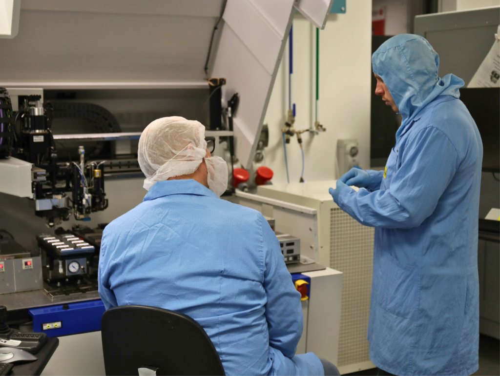
If you’re progressing a project in-house but need help with part of the process – design, assembly, testing, metrology, validation or troubleshooting – we can step in where needed. You define the scope; we deliver dependable, high-quality execution.
Examples include:
- Consulting on, designing and setting up custom packaging processes
- Optical fibre and PIC coupling
- Specialist die attach and flip-chip processes
- Interposer design, preparation and metallisation
- Thermal and thermoelectric modelling
- Performance verification and validation
- Reliability testing
- Failure analysis and problem resolution
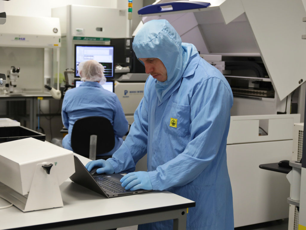
We integrate seamlessly with your workflow, providing the expertise and equipment not typically available in standard industrial settings.
For projects where something hasn’t gone as expected and you need help understanding or troubleshooting.
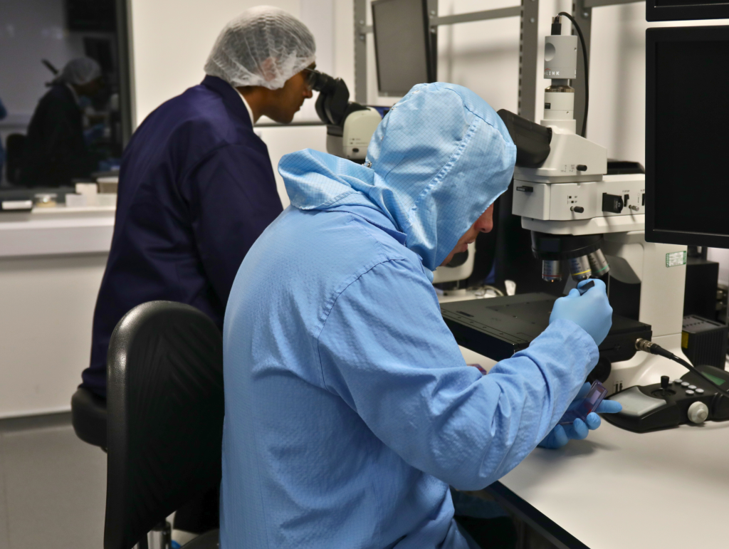
We work with you to investigate issues, identify root causes and provide practical, actionable solutions. Using our in-house lab capabilities and our network of metrology and testing partners, we deliver fast, reliable insights so you can keep your project moving forwards.
This includes:
- Root cause investigation
- Access to a wide range of metrology techniques, for example:
- Electrical, thermal and mechanical testing
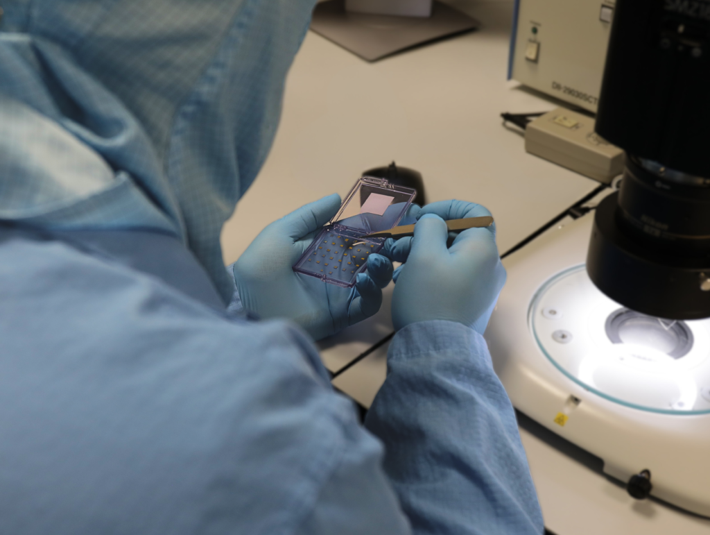
- Microscopy and imaging
- X-ray tomography
- Independent quality and performance testing
- Data analysis and reporting
- Recommendations for design improvements
- Collaboration with your suppliers, as required
Coming soon… For low-volume builds, R&D and pilot runs.
STARPACK is a modular platform for integrating electronic and photonic chiplets into a single system-in-package. Currently in development as part of an ongoing Innovate UK project, it offers a flexible, cost-effective alternative to fully custom packaging solutions.
Created alongside industry experts, this platform is designed to overcome the limitations of legacy packaging and accelerate development cycles.

Our capabilities
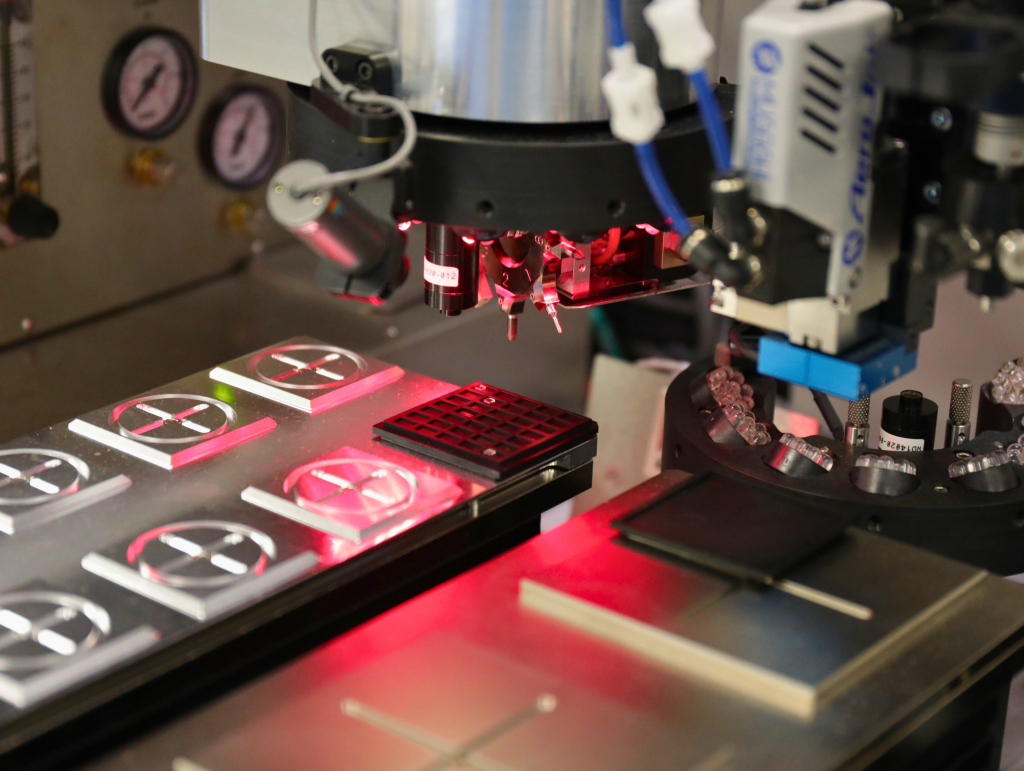
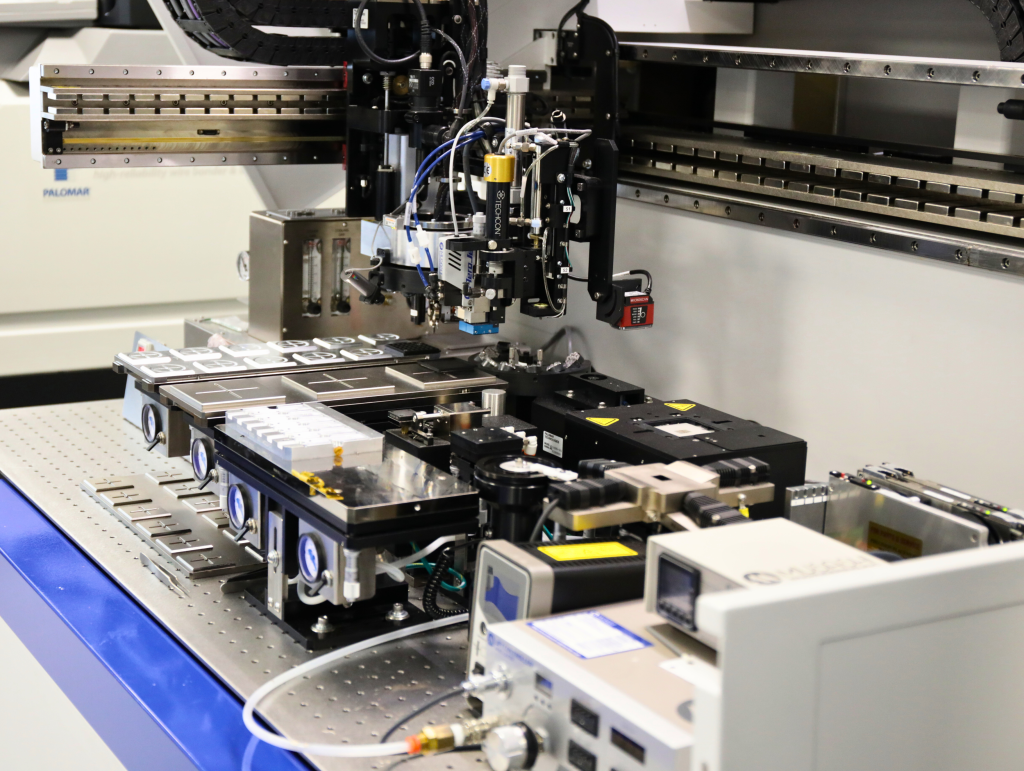
We offer advanced processes and facilities that are often unavailable in standard industrial environments, ideal for prototype, R&D and small-scale production.
Electrical interconnects
- High frequency, microwave and RF interconnects
- High spatial density area-array attach, including custom interposer design, fabrication and flip-chip bonding
- Cryogenic-compatible processes and materials, including indium
- Individual die preparation (under-bump metallisation) and attach
- Wafer-level processes including redistribution layers (RDL), solder deposition and passivation
Optical interconnects
- Low-loss interconnects
- Cryogenics
- Multiple, high-density optical interconnects
- Sourcing fibre coupler and array attachments
- High-density and miniaturised optical benches
Reliability testing
- Accelerated life testing
- Thermal cycling
- Damp heat
On-site resources
- Failure analysis lab (X-ray, SEM with EDS, optical microscopy, pull testing)
- Flexible assembly and processing equipment for fast turnaround
Ready to get started?
Explore how Hybrid Integration can help bring your project to life.